Microsampling application for semiconductor customers
With the growing demand for semiconductors around the world, inquiries and requests from customers related to foreign matter analysis has been increasing recently.
Today, we would like to introduce various applications based on our customer’s inquiries
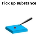
Pick up substance
Application
| ●Clean up fine contamination on a wafer ●Repair of fine wiring(Connection/Disconnection) ●Isolation of defects in LCD/OEL for analysis ●Isolation of defects adhered to substrate for identification ●Isolation of defects from image sensor for analysis ●Isolation of defects on photomask and grating for analysis |
 |
Product
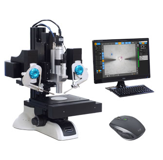 Manipulator Axis Pro |
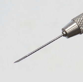 Tungsten probe Tungsten carbide tools |
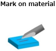
Mark on material
Application
| ●Mark around defects on a wafer for SEM ●Mark around FIB location (Preparation before FIB) ●Cut and connect wiring in a circuit ●Scribing substrate for cleavage |
 |
Product
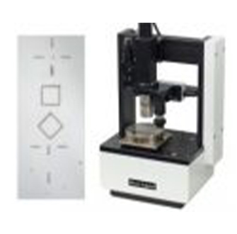 Marking system D-MARK |
 Manipulator Axis Pro |
 Knife Edges Tungsten carbide tools |
FIB lift-out
Application
| ●FIB lift-out ●Replace FIB thin sample and attach outside SEM(Saving chamber time) ●Sampling remotely under special environment (such as inside a glove box). |
 |
Product
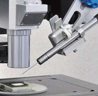 Super Fine Pitch Rotator |
 Manipulator Axis Pro |
 Knife Edges Tungsten carbide tools |
Grab and adsorption of tips
Application
| ●Relocate diced test piece without damage ●Place small electric component on designated area ●Grab fine wire for adhesion or welding |
 |
Product
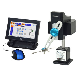 tand-alone manipulator Quick Pro |
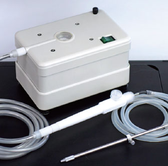 Vacuum adsorption tool set |
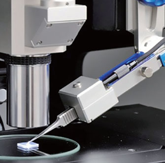 Micro tweezers |
Electrical probing
Application
| ●Probing between electrodes on substrate or circuit. ●Contact 1μm width pad with probe ●Measurement for particle of battery material |
 |
Product
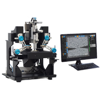 Probe station |
 Electrical probe holders |


